The Inner Workings of the Kaufman Ion Source
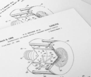
In simple terms, a Kaufman ion source operates as follows:
- The filament cathode thermionically emits electrons.
- The electrons are attracted to the positively biased anode. However, their path is not straight but rather the electrons drift in a cycloidial path due to a confining magnetic field.
- As the electrons travel, they impact a neutral atom (molecule) from a working gas fed into the discharge chamber, resulting in ionization.
- The ionization cascade establishes a high-density plasma in the discharge chamber.
- The plasma is elevated to a positive potential with respect to ground by the biased anode.
- At the ion optics, the plasma is contained within the discharge region chamber by the multi-aperture screen grid. However, when a negative bias is applied to the accelerator grid, an electric field is established and it extracts ions from the plasma discharge.
- The extracted ions flow through the grid apertures on their way to form an ion beam.

Superior Systems Enabling Atomic-Level Control
Companies depend on KRI® technology when high-purity material processing is the objective. Implemented in vacuum environments, it is used in the deposition of thin films and etching of surfaces.
Our solutions enable the fabrication of structures with critical dimensions ranging from the micrometer to sub nanometer scale. Capable of extremely high precision, these products are engaged in creating material systems and surface features with atomic-level control.


